
Wafer Packaging Systems | ITW EBA - Semiconductor Solutions
ITW EBA wafer packaging systems provide cost-effective secure storage and transport solutions for 150mm to 300mm semiconductor wafers. Trusted by industry leaders.
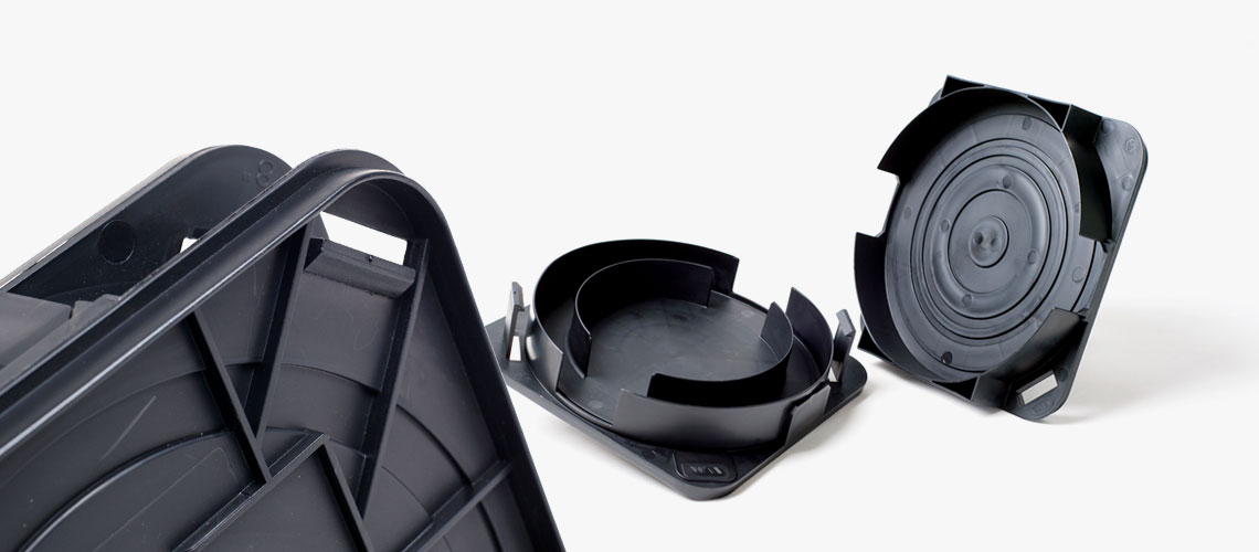
Wafer Packaging Systems
ITW ECPS
Our wafer packaging systems product line is your cost effective solution to secure storage and transport of semiconductor wafers, ranges from 150 mm to 300 mm.
 Download
Hot Products
How can you ensure your semiconductor wafers remain protected during storage and transport without compromising your budget?
ITW EBA's wafer packaging systems deliver cost-effective protection for your critical semiconductor inventory. Our proven solutions for 150mm to 300mm wafers combine secure containment with economical design, reducing damage-related losses while maintaining the highest quality standards. With five decades of IC packaging expertise, we understand the precision requirements of semiconductor operations and provide systems engineered for reliability and performance.
Backed by Illinois Tool Works' global resources and commitment to quality, ITW ECPS wafer packaging systems represent a strategic investment for semiconductor manufacturers, foundries, and logistics providers seeking reliable, economical solutions. Whether you require standard packaging configurations or custom-engineered systems tailored to specific operational requirements, our comprehensive product line addresses the full spectrum of wafer handling needs. Contact ITW EBA today to discover how our specialized wafer packaging expertise can optimize your semiconductor storage and transport operations while reducing costs and improving operational efficiency.